Surface Treatment – Plating / TGV
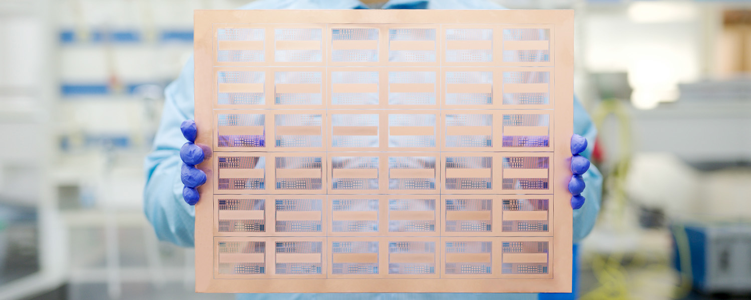
Metallization on Hard-to-plate Materials
In response to the development of communications technology, the design of electronic products is significantly changing. Along with that, various basic materials for electronic products are being developed and started to be used to satisfy diversified requirements. We are happy to serve our customers by forming a metal film on promising materials in the field of electronics.
Inorganic materials: Glass, Ceramics
Organic materials: ABS, Liquid crystal polymer, Cycloolefin polymer, Nylon, etc.

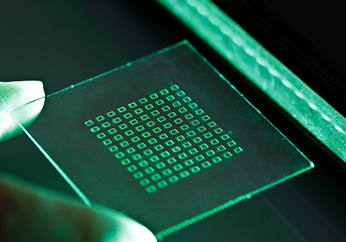
1. Plating on Glass、GWC(Glass Wet Cu Plating)、TGV(Through Glass Vias)
GWC:
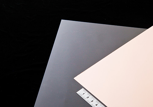
The current method for forming metal films on glass substrates presents several challenges, such as weak adhesion strength, difficulty achieving uniform coating on three-dimensional molded objects, the need for surface roughening, and issues with heat resistance. Our newly developed processing technique, "GWC," is Koto Electric's proprietary metal coating formation process that significantly addresses these challenges. This wet method allows the formation of Cu (copper) coatings with strong adhesion on various types of glass without roughening the glass surface.

Adhesion strength:
By applying copper plating on various types of glass using the GWC process, the adhesion strength shown in the table below can be achieved. An adhesion strength of 0.8 kN/m or higher is obtained on alkali-free glass, making it suitable for adoption as a glass substrate. Furthermore, by forming a copper coating on quartz, it is expected to be used for high-frequency substrates.
| Alkali-free Glass | 0.8 kN/m |
|---|---|
| Borosilicate Glass | 0.5 kN/m |
| Quartz | 0.3-0.4 kN/m |
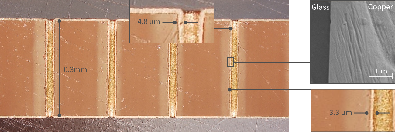
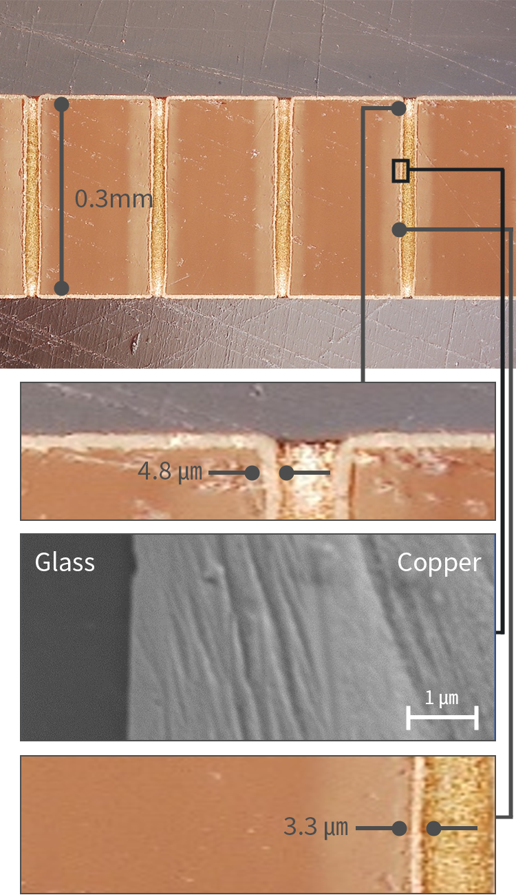
TGV substrate with Cu plated coating coverage:
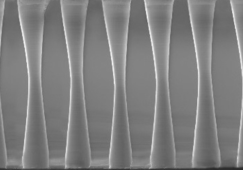
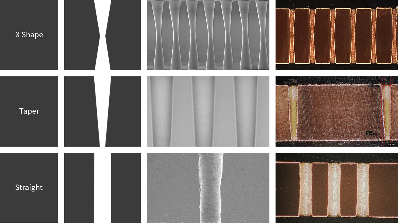
TGV have a variety of via shapes. The GWC process, utilizing a wet method, enables uniform copper deposition on vias regardless of their shape. It supports plating with an aspect ratio of up to 20.

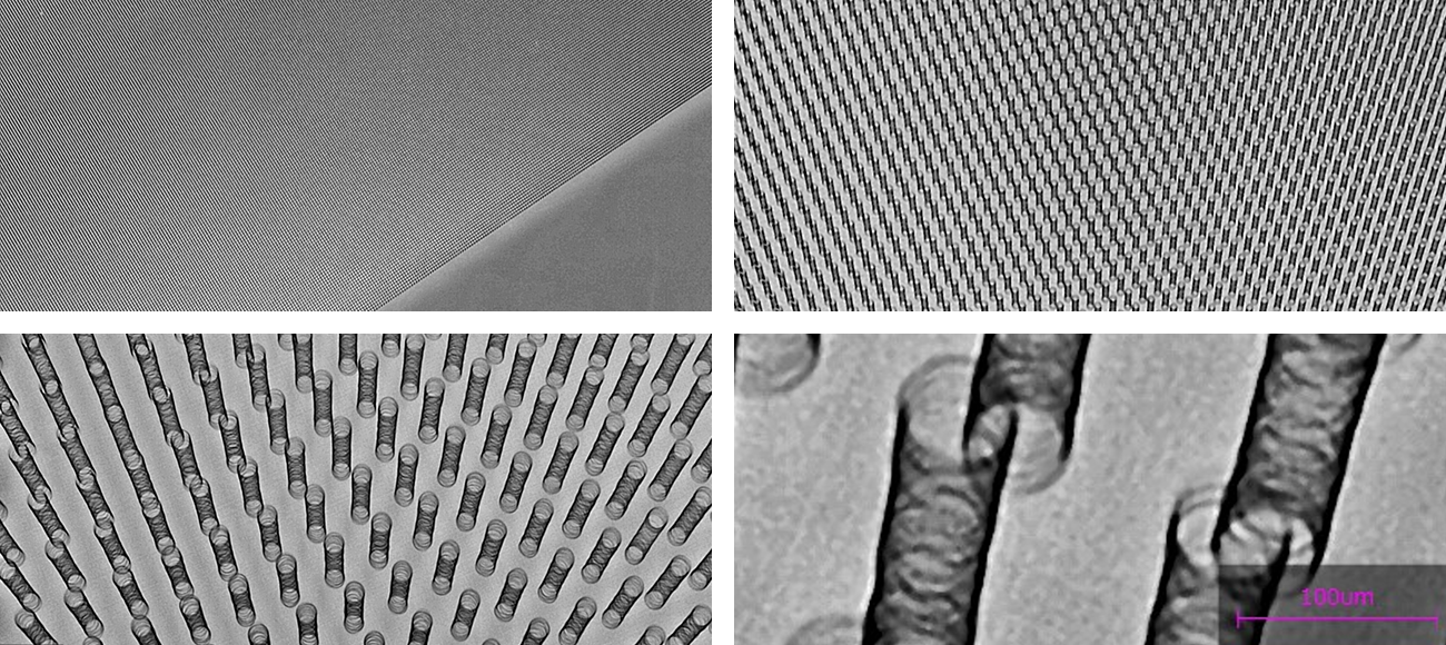
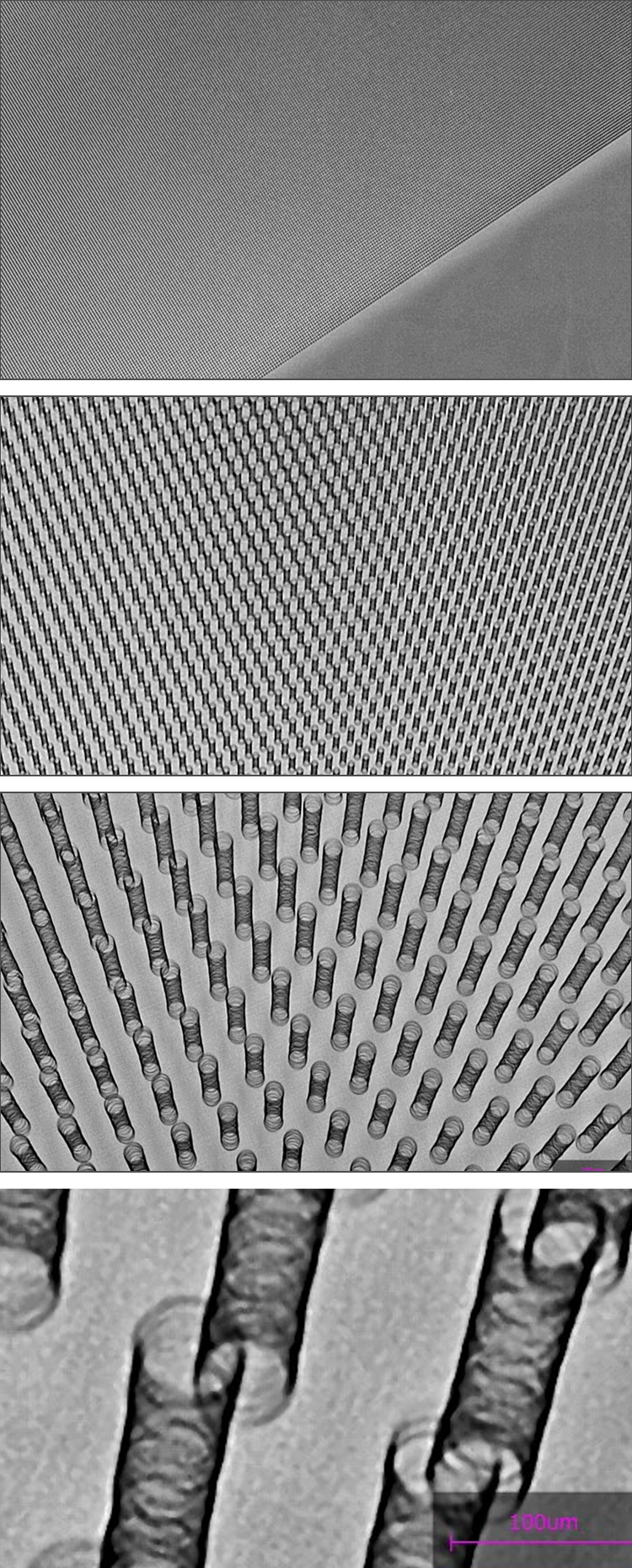
Application to high-density TGV substrates:
This is an image of a TGV substrate observed using X-ray CT after copper plating. Copper can be uniformly deposited on high-density TGV substrates.
Fine line pattern:
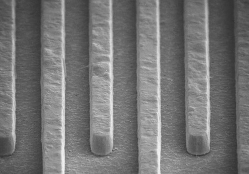
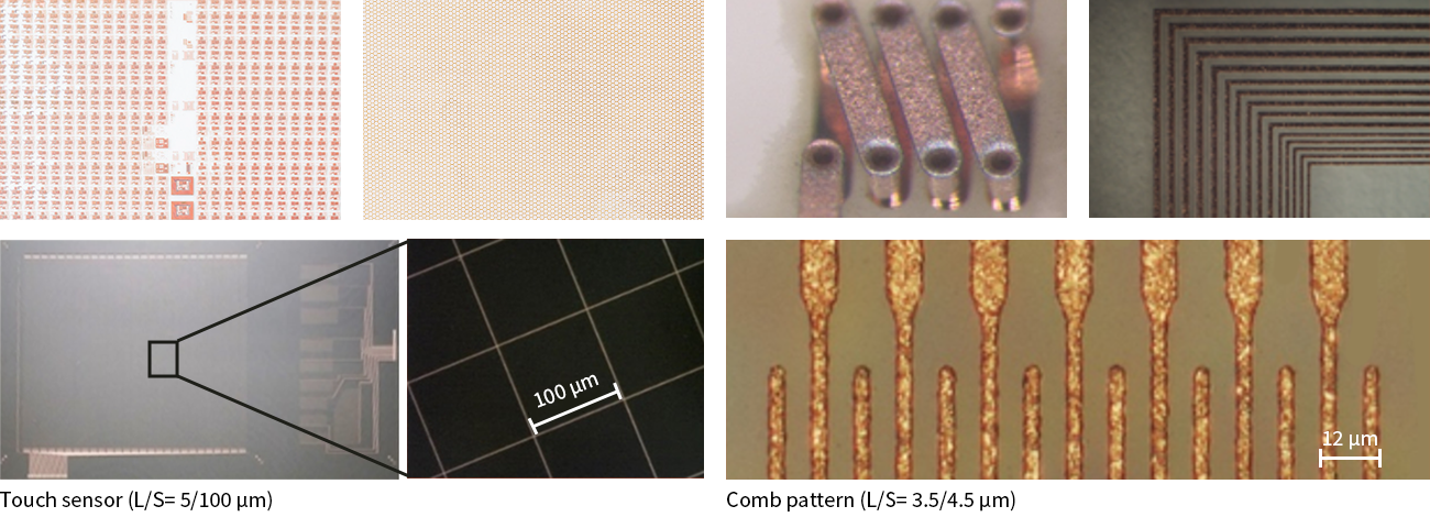
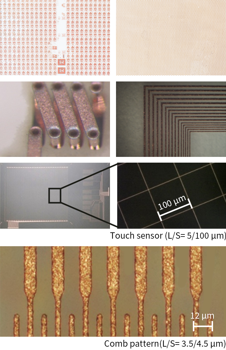
It enables the formation of fine patterns without damaging the smooth surface of the glass. Additionally, the front and back patterns are securely connected through the TGV.
Plating on glass tubes:
Even on irregularly shaped materials such as glass tubes, it is possible to form conductive and reflective coatings on both the inner and outer surfaces.

Plating on extremely fine glass materials (powder):
It is possible to apply a uniform conductive coating to powder materials with diameters ranging from a few micrometers to several tens of micrometers, such as resin and glass.

2. Metallization (Plating) on Ceramics
Plating of Ni/Sn, Ni/Au, Ni/Ag, etc. is available on the Ag-metallized (printed) ceramics.

Proven Applications

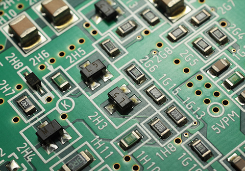
Touch panel
Interposer
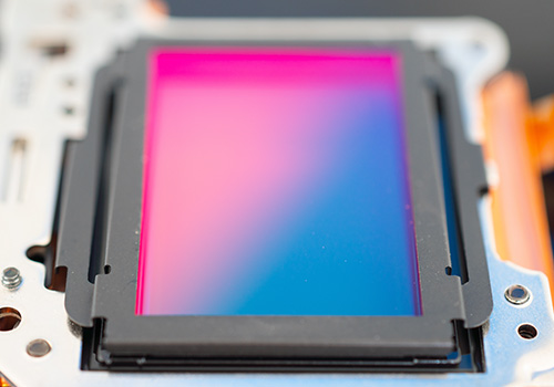
Image sensor
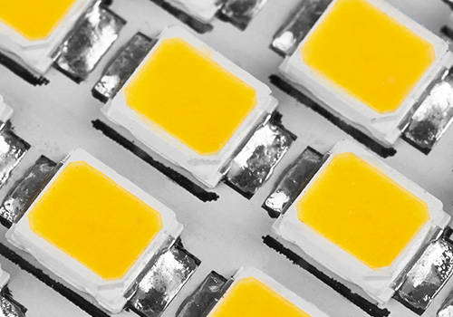
LED

High-frequency antenna

RF device
Examples of Promising Applications

5G remote (online) surgery

5G vehicular communication
Plating on Minute and Small Parts
Electronics components are being required to be downsized and multifunctional to cope with the development of smart phones, tablets, automobiles, and robots. It is also required to improve the production efficiency and quality stability of the electronics components. Koto has the technology to plate on minute parts as well as the proven barrel plating technology on small components. We are happy to receive small-lot prototype orders not to mention large quantity orders where we plate as many parts as possible at one time.

Plating type
Nickel Plating
| Features | ・Whitish silver finish ・High corrosion resistance ・Proper hardness (Matte: approx. HV 200, Semi-bright or bright finishes: approx. HV 500) ・Stress: Normally, tensile stress ・Changes in bath composition, additive concentration, and electrolysis condition can add flexibility to and reduce stress in films. Films can have a wide range of physical and mechanical properties. |
|---|---|
| Bath types | ・Matte nickel plating bath (Watts bath) ・Semi-bright nickel plating bath (Watts bath) ・Wood's nickel strike bath ・Nickel sulfamate bath |
| Process of manufacture | ・Barrel plating ・Rack plating |
| Uses | Corrosion prevention and undercoat for gold plating for the hermetic seals (steels) used in electronics components for automobiles, aircrafts and pressure sensors. |
Gold Plating
| Features | Gold plating in general ・High corrosion resistance ・Good electrodeposition property ・Low contact resistance, Good electrification characteristic, Easy soldering ・Hard gold plating Au:99.7%, Approx. Hv 200, Good wear resistance ・Soft gold plating Au:99.99%, Approx. Hv 80, Good bondability |
|---|---|
| Bath types | ・Strike gold plating (Acid bath) ・Hard gold plating (Acid bath, For contact materials and connectors) ・Soft gold plating (Middle bath, For bonding) |
| Process of manufacture | ・Barrel plating ・Rack plating ・Selective gold plating using in-house-designed machine |
| Uses | Bonding of hermetic seals used in electronics for automobiles, aircrafts and pressure sensors as well as finish plating for connectors. In-house-designed selective gold plating machine is used for plating. |
Copper Plating
| Features | ・High corrosion resistance ・Soft and easily spreadable ・High conductivity of heat and electricity ・Widely used as an undercoat for various platings |
|---|---|
| Bath types | ・Strong alkaline bath ・Acid bath ・Pyrophosphate bath |
| Process of manufacture | ・Rack plating ・Barrel plating ・Hook plating |
| Uses | Copper plating is widely used for various materials. A suitable bath type will be selected according to the usage. Copper plating can be used for the materials of electronic substrates and to improve designability. |
Electroless Nickel Plating
| Features | ・Unlike electroplating, power supply not needed ・Contact on a substrate not needed ・Uniform deposition ・High coating hardness, Good wear resistance (After Ni-P plating: Approx. Hv 500, After heat treatment: Approx. Hv 1000, After Ni-B plating: Approx. Hv 700 to 800) ・Less pinholes than those by electroplating ・Stress: Normally, compressive stress ・Good solderability and bondability (Ni-B) |
|---|---|
| Bath types | ・Electroless nickel-phosphorus plating bath (Middle phosphorus bath) ・Electroless nickel-boron plating bath ・Electroless nickel-phosphorus plating bath (Lead-free bath) ・Electroless nickel-boron plating bath (Lead-free bath) |
| Process of manufacture | ・Barrel plating ・Rack plating ・Others |
| Uses | Corrosion prevention and undercoat for gold plating for the hermetic seals used in electronics components for automobiles, aircrafts and pressure sensors. |
Electroless Gold Plating
| Features | ・High corrosion resistance ・Good electrodeposition property ・Low contact resistance, Good electrification characteristic, Easy soldering ・Electric contact not needed ・Applicable to the high-density wiring of electronic components |
|---|---|
| Bath types | ・Displacement electroless gold plating bath ・Thick plating type displacement electroless gold plating bath ・Autocatalytic electroless gold plating bath |
| Process of manufacture | ・Barrel plating ・Rack plating ・Others |
| Uses | Plating on the connectors of direct view filament display for aerospace. |
Tin Plating
| Features | ・Good solderability ・Bath type selectable corresponding to material ・High lubricity ・Environmentally friendly, Compliant with applicable laws and regulations ・Less likely to develop whiskers |
|---|---|
| Bath types | ・Neutral tin plating bath ・Acidic tin plating bath |
| Process of manufacture | ・Barrel plating |
| Uses | Plating on the contacting points of capacitors and inductors. |
In addition to the above types of plating, solder plating and Ag plating are available. We are happy to suggest you the best plating options to respond to your requirements.
Processing Line, Equipment, Analysis

Our equipment and plating line can handle your requirements from beaker testing for a small amount of sample material to plating on a large material.
Analysis, Inspection
List of Equipment and Facility
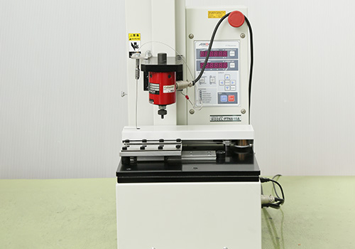
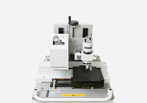
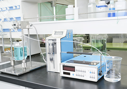
Film hardness tester / Adhesion strength tester / Particle counter / Pilot line / Inductively Coupled Plasma Optical Emission Spectrometer (ICP-OES) / Scanning Electron Microscope (SEM) / Digital microscope / High Accelerated Stress Test (HAST) chamber / Solder checker / X-ray fluorescence film thickness meter / He leak detector / Cyclic Voltammetry Stripping (CVS) analyzer / Spectrophotometer / High power UV irradiation equipment / Box furnace
Click here for inquiries about each department and product

